Applications
DRAMMST Powers Tomorrow’s Best Memory Architectures
MST allows DRAM designers to reduce chip size without moving to a new technology node, enabling product enhancements and cost reductions within a current design or for new designs. With MST in place, new design features are available that allow designers to optimize supply voltage (VDD) to reduce both active and standby power for mobile products and for power-hungry applications such as data centers.
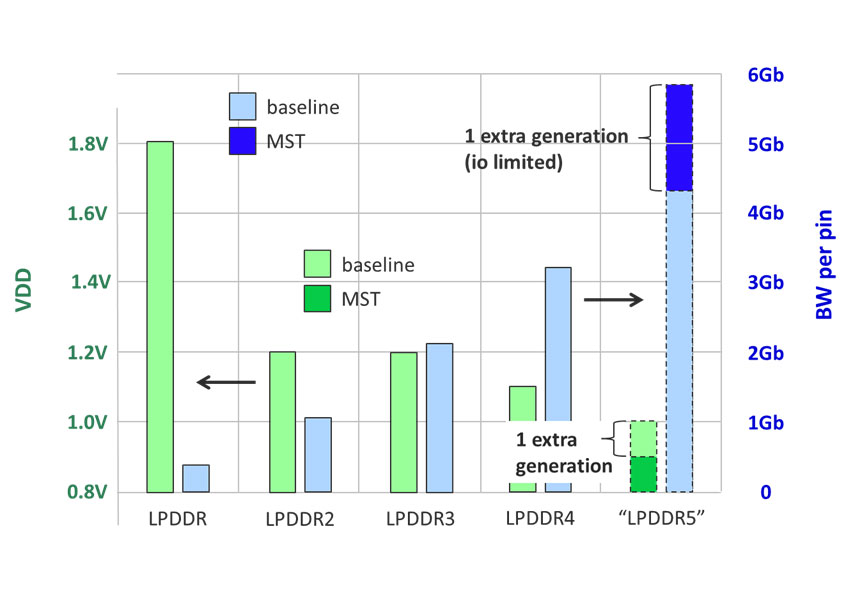
Insertion of MST in next generation chip designs enables circuit designers to reduce supply voltage (VDD) even further and optimize read/write conditions to modern LPDDR 5 requirements. Third party DRAM product design experts estimate that MST improvements represent up to one node of incremental product performance.
The MST “technology tool box” allows for significant enhancements in Gm (50%), Idlin and Idsat enhancements, gate leakage reduction (2.7x for HKMG), 50% mismatch reduction (e.g. sense amp) and reliability enhancements in TDDB/NBTI (Poly-SiON) & PBTI (HKMG) allowing for up to 100mV overdrive. Successful integration of MST into DRAM products has been estimated to provide significant performance, power, area and cost savings similar to those shown below:
New DRAM Designs and Chip Size Reduction for Mature Products
Taking advantage of the reduced supply voltage and overdrive capabilities enabled by MST, estimates indicate that DRAM designers have the ability to increase the bandwidth of DRAM products while reducing their voltage


