Technology
MST AdvantagesPerformance Enhancing Materials
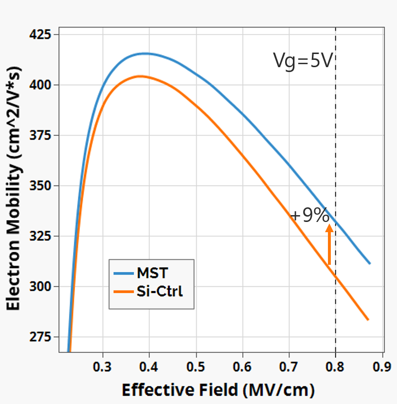
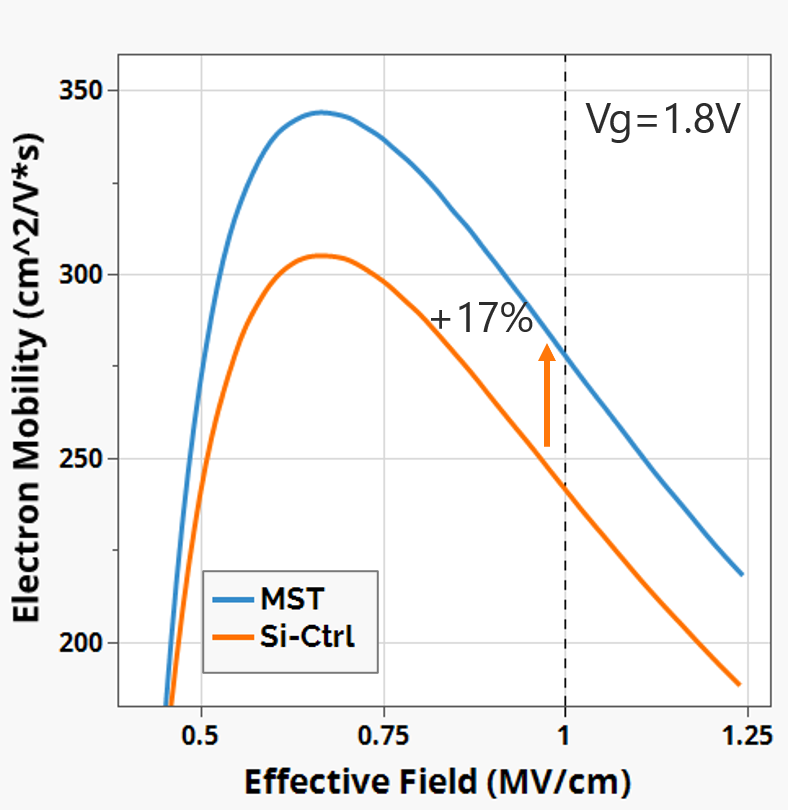
MST enables increased carrier mobility and drive current. These benefits are applicable to a variety of IC types. Drive and effective current increases of 10%-20% and improved mobility at high and low fields have already been demonstrated during third party evaluations.
5V NFET Mobility
1.8V NFET Mobility
Lower Power Means Greener Electronics
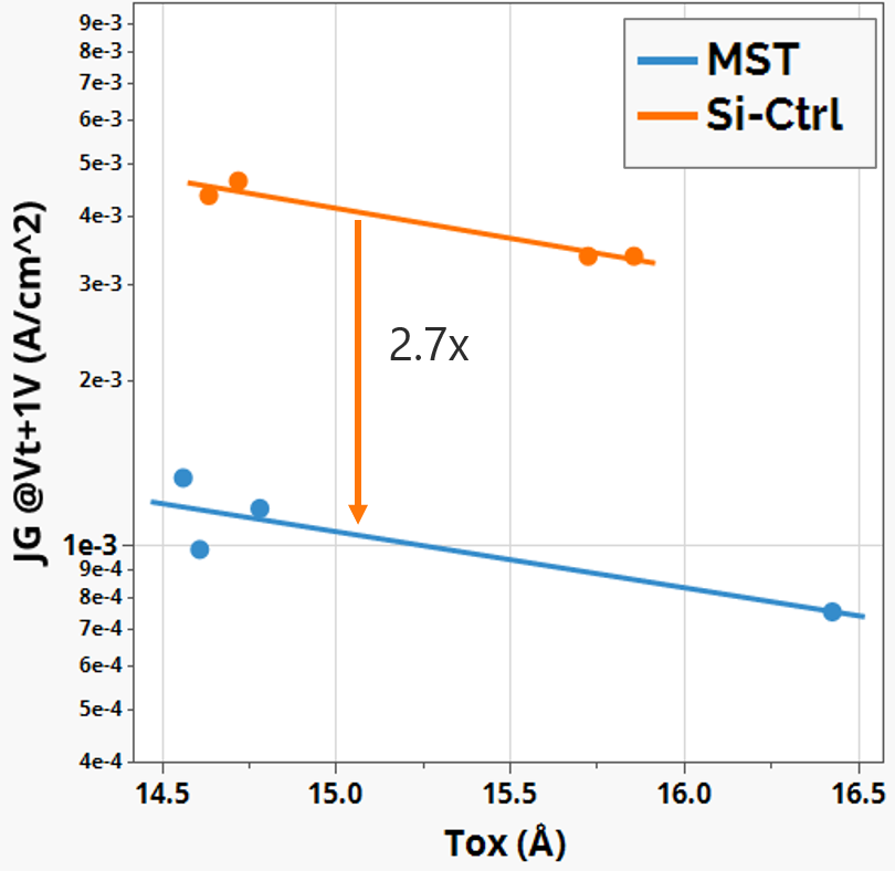
In the same way that MST can be used to improve performance, it can also be used to lower power consumption by reducing leakage. One of the biggest challenges for semiconductor designers is to deal with increased gate leakage at smaller process geometries. MST® can help. Gate leakage reductions greater than 60% have been demonstrated during third party evaluations by impeding unwanted transistor current flow in the vertical direction. Another way power consumption can be lowered is by trading off some of the performance enhancements mentioned above and reducing voltage.
Reliability Leads to a Longer Life and Higher Performance
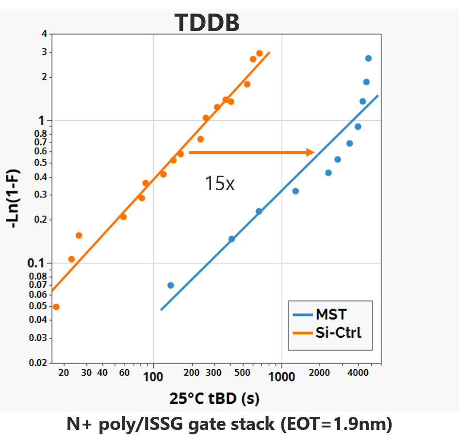
When most people think of reliability, they think of products lasting longer. For chip designers, it means they have more options. They can either extend the expected lifetime of their designs, or run them at a higher voltage while keeping the same lifetime which brings them higher performance. Atomera accomplishes this by improving the Gate Oxide Integrity of transistors. Measurements at our lab partners support improved reliability, potentially allowing further drive current increase by over-driving transistors.
Lower Cost is Always Better
MST can be used to lower costs in multiple ways. Generally, when chips are designed to run at lower power levels, die area can be made smaller. So as MST® lowers power, it also can reduce die size. In addition, MST® has the ability to increase manufacturing yield which means fewer “bad” die are produced. Both smaller die size and improved yield help to lower chip cost.
Reducing the Variability Problem
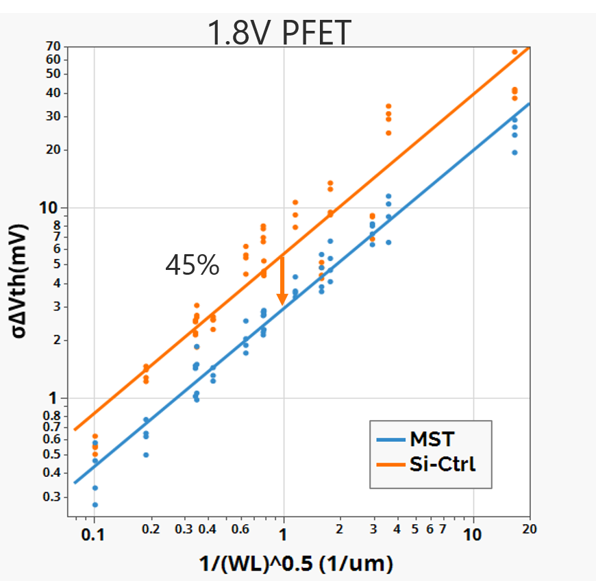
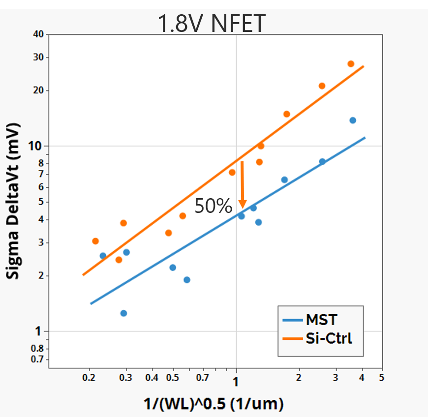
As chips continue to shrink, random differences in the placement of an atom can cause large variations in electrical properties. This increase in variability is a major problem in semiconductors which Atomera helps to mitigate. MST’s improved channel doping, through a super steep retrograde profile, reduces random dopant fluctuation and delivers increasingly important benefits in the form of reduced variability in threshold voltage “Vt” and improved matching. Up to 50% reduction in Vt variability and improved transistor matching have been demonstrated during third party evaluations.
MST matching data 1.8V PFET
MST matching data 1.8V NFET
Additional MST Advantages
‘Silicon‐on‐Silicon’ – Additive Benefits
MST is a single crystal ‘Silicon-on-Silicon’ solution that provides multiple benefits through a relatively simple modification to the standard CMOS manufacturing flow; one that can be used across multiple process technology “nodes” and a variety of IC product generations. The technology is also additive and complementary to SOI and strain technology.
High Benefit / Cost Ratio
MST lends itself to further enhancement and customization, as the epitaxial layer design can be optimized for specific applications based on performance priorities and cost targets. With a low fabrication process flow cost for the single film insertion, MST delivers a high benefit to cost ratio across multiple products.

