

Who we are
We are a transistor materials innovator
MST is a thin film material which enables higher performance transistors, implemented on epi reactors readily available in today's semiconductor fabs.
What we make
A quantum-engineered epitaxial silicon film
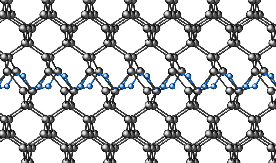
Atomera's patented Mears Silicon Technology™ (MST®) inserts partial monolayers of unique elements in Epitaxial Silicon that control dopant movements through subsequent thermal processing improving the transistor: better performance, lower power and lower cost for logic, DRAM, power, RF and GaN devices.
Full node
of PPAC improvement without physical scaling
No design rule changes
Dopant engineering by one key unit process change
Existing HVM tools
MST demonstrated on epi reactors from all 3 major tool vendors
402
issued and pending patents worldwide (June 30, 2025)
PatentsPRIMA & SELECTA – MST application methods
In the substrate, or in the device
MST Engineered Starting Substrate
MST grown as a blanket film across the starting wafer, creating an engineered substrate. Transistors and devices are then grown on top.
applicationsMST Integrated into devices
Quantum-engineered epitaxial silicon, grown selectively or non-selectively, inside or on top of existing device structures.
applicationsWhat MST does
Dopants stay where devices need them for optimal performance
MST creates a thermodynamically stable environment that blocks dopants. Engineered dopant profiles form, and survive high thermal budgets.
Diffusion blocking
MST traps the silicon interstitials that carry dopants, so dopants stay put through high thermal budgets.
Dopant profile engineering
Profiles built for each device: lower resistance, abrupt interfaces and new transistor designs.
Smoother Si/SiO₂ interface
About half the surface-roughness scattering, for higher carrier mobility at high gate fields.
Better gate oxide
A better silicon/gate-oxide interface: lower gate leakage and longer device life.
Lower Schottky barrier
260 mV lower barrier at the metal/silicon contact, for lower contact resistance.
Applications targeted
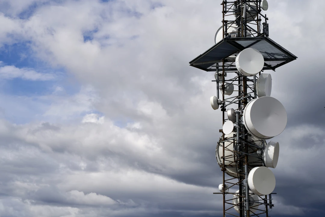
One technology platform customized for each transistor improves performance across six product families, from leading logic to DRAM to NAND to Power, GaN and RF, serving AI infrastructure, mobile and telecom.

Six product families
Markets

AI Infrastructure

Mobile
Telecom
Infrastructure
















AI Infrastructure
Mobile
Telecom
Infrastructure
Customer engagement
From simulation to your silicon
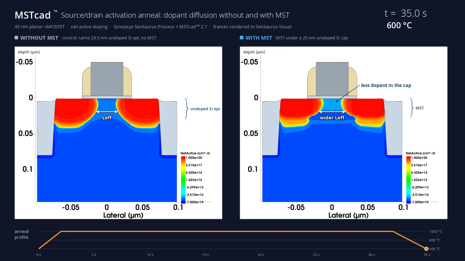
MSTcad™
Leverage our silicon-fitted TCAD to accurately predict MST performance on your own devices and processes, before wafers are run.
Integration on your devices
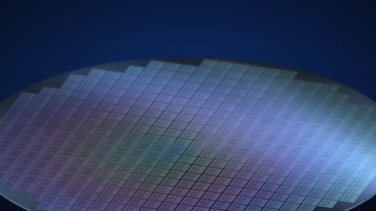
Our integration experts work with customers to optimize MST into your devices and process flow, delivering peak device performance.
Talk to us
Work with us
Partner with Atomera
Evaluate MST in your own process and devices with Atomera's engineering team.
Contact us