

Applications
Transistors are everywhere
Quantum-engineered MST epitaxial silicon solves critical bottlenecks, enabling industry-leading semiconductor product performance for each application.
One film, many devices
MST improves transistors enabling device scaling & unlocking performance gains
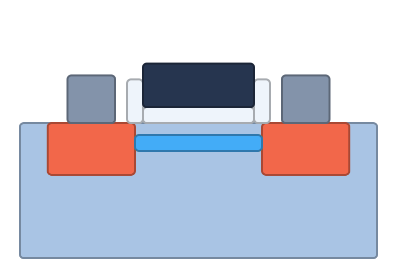
Planar CMOS
Mature nodes: dopant control, less variability
Explore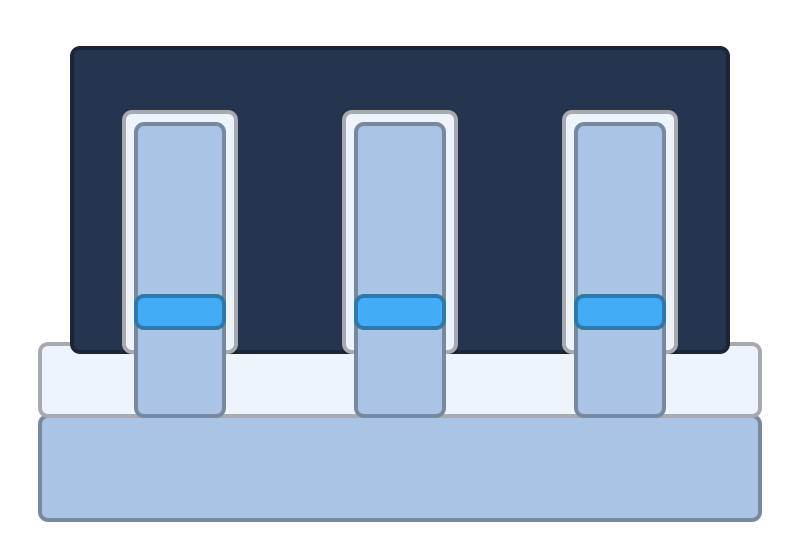
FinFET
Fin channel: leakage and variability control
Explore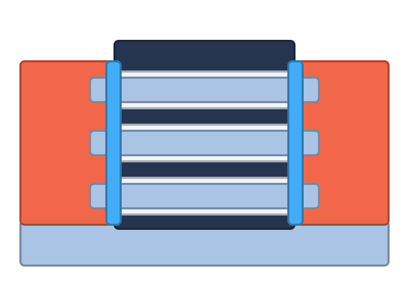
GAA Nanosheet
Blocks S/D dopant diffusion; cuts RDF
Explore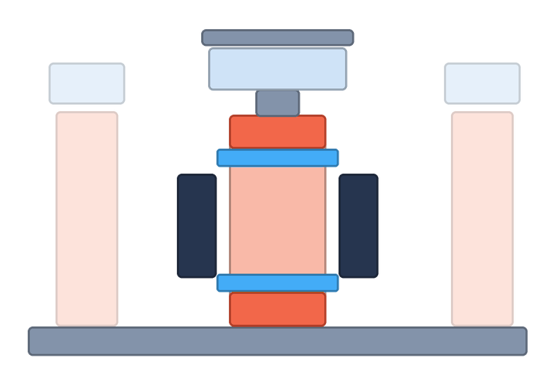
DRAM FETs
Sense-amp variability; 4F2 vertical channel
Explore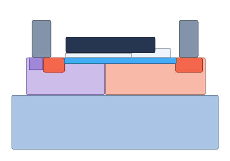
LDMOS (BCD)
Lower Rsp, higher breakdown margin
Explore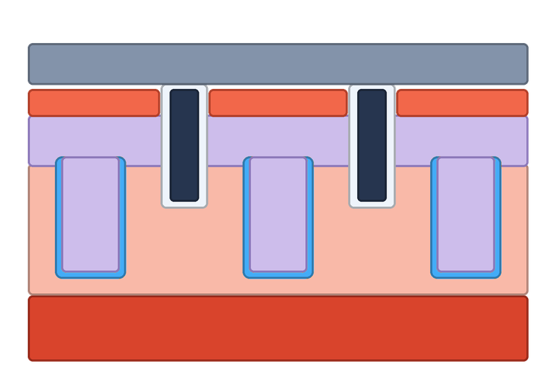
Trench MOSFET
High-voltage, high-speed TrenchFET
Explore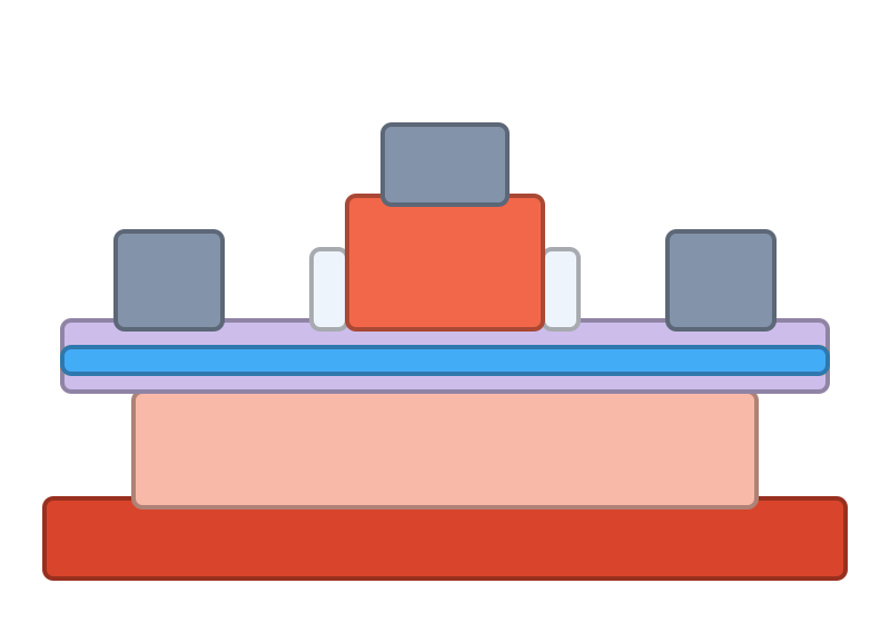
HBT (Bipolar)
High-frequency, high-speed bipolar
Explore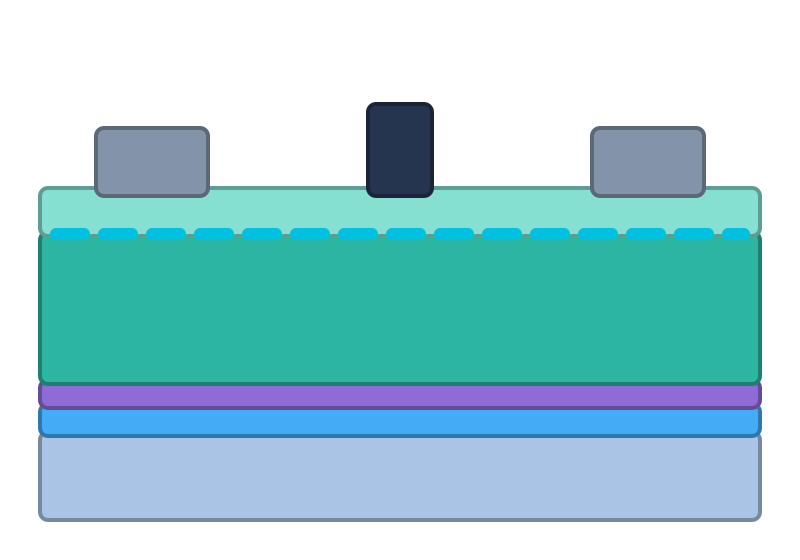
GaN-on-Si HEMT
Suppresses the Si/GaN parasitic channel
Explore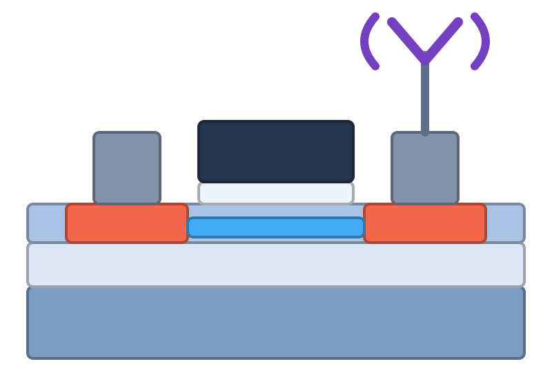
RF-SOI FET
Antenna switches and low-noise amplifiers
ExploreWhere MST is used
Applications
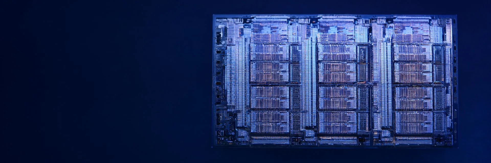
Leading Logic
Gate-all-around transistors with steeper junctions, a lower-resistance contact and a better gate stack.
Explore
DRAM
A pre-doped MST starting wafer for 4F² vertical-channel DRAM: 2.5–3× read/write current in TCAD simulation.
Explore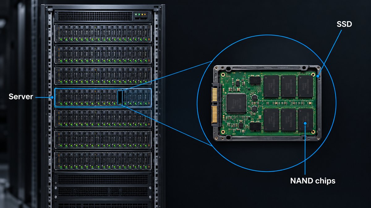
3D NAND
HV CMOS with better performance leveraging MST Power Devices know-how.
Explore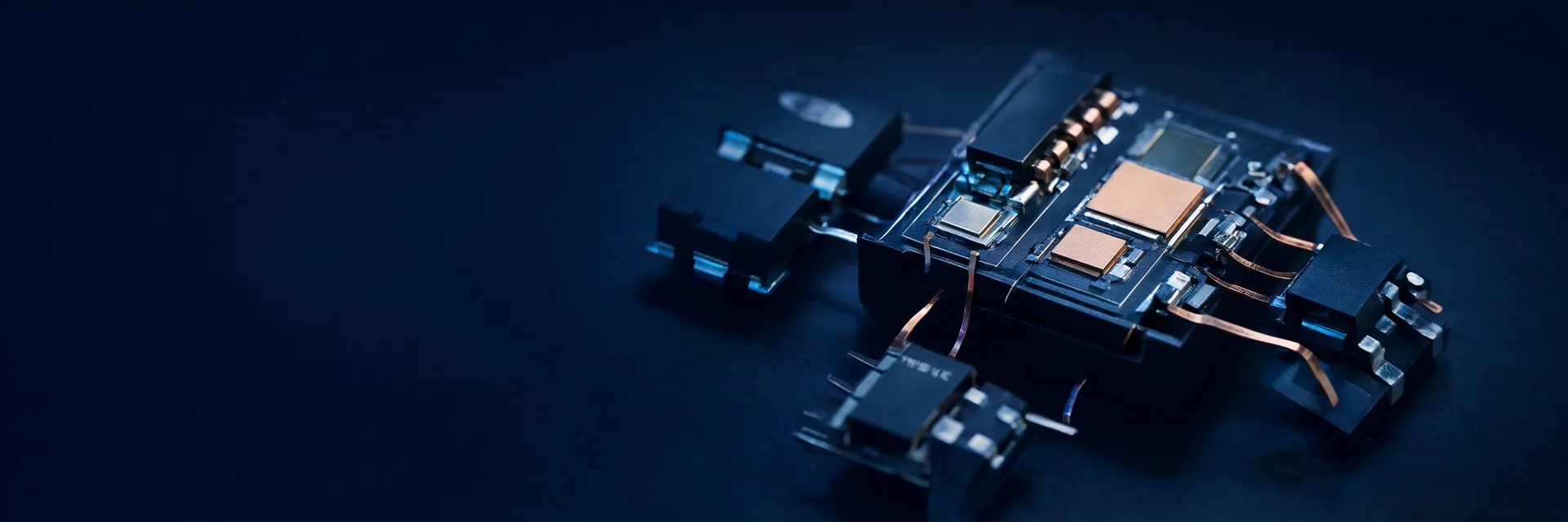
Analog & Power
Lower on-resistance at the same breakdown and reliability, from 5 V BCD switches to LDMOS.
Explore
GaN-on-Si
A better GaN crystal for power, and low-loss, highly linear GaN-on-Si for RF, from one thin MST layer.
Explore
RF-SOI
Lower Ron·Coff, leakage and cleaner harmonics for RF switches, on thinner top silicon.
Explore
Work with us
Partner with Atomera
Evaluate MST in your own process and devices with Atomera's engineering team.
Contact us