
Technology
MSTcad™
Atomera's TCAD library for Synopsys Sentaurus: model MST in your own process and device flow.
MSTcad™ in action
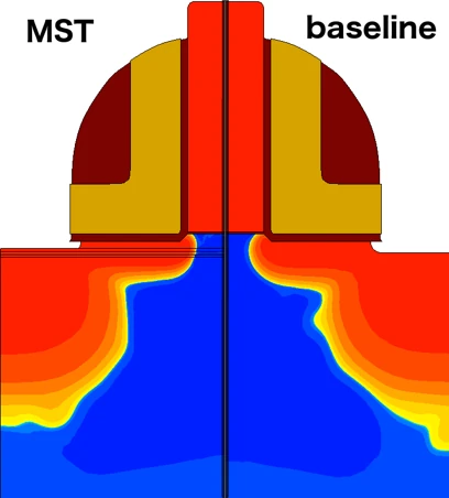
Source/drain anneal of a 45 nm transistor, with and without MST
Two identical 45 nm transistors, one with MST and one without, through the same source/drain anneal. Colour shows the dopants.
MSTcad™ simulation in Synopsys Sentaurus Process. Simulation results, not measured data.
how MSTcad™ works
Models fitted to real silicon
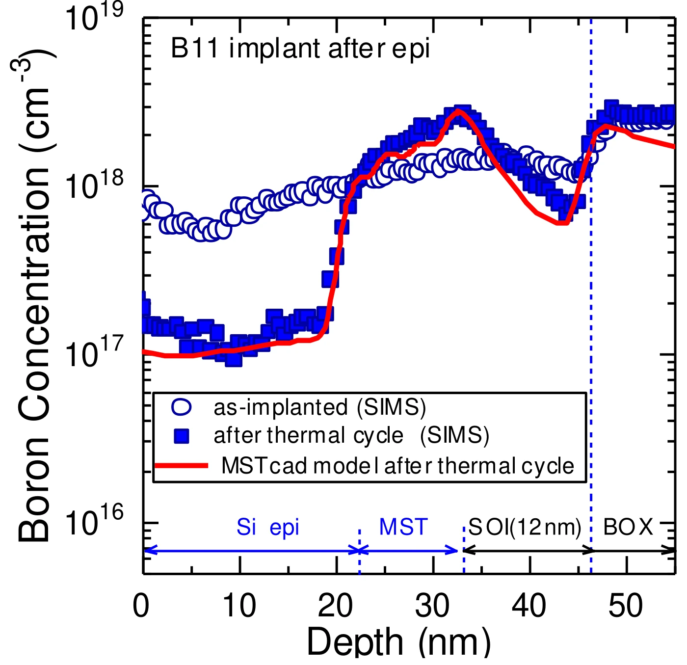
MSTcad™ models each MST layer as a thin interface inside Synopsys Sentaurus, where silicon defects and dopants are trapped and released. It runs inside your own process flow, so every implant and anneal sees MST. The models are fitted to measured silicon data (SIMS profiles), so simulations match what the fab sees.
inside a customer flow
STEP 1
Deposit
Add the MST film to your structure, where the epi is grown.
STEP 2
Process
Run your own implant and thermal steps with MST physics on.
STEP 3
Simulate the device
See MST's effect on your device before wafers are run.

Work with us
Partner with Atomera
Evaluate MST in your own process and devices with Atomera's engineering team.
Contact us