
Executive summary
Five properties, one film
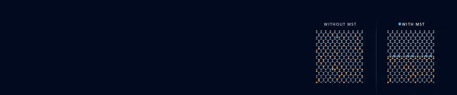
MST creates a thermodynamically stable environment that blocks dopants. Engineered dopant profiles form, and survive high thermal budgets.
Diffusion Blocking
Holds dopants in place through high thermal budgets, including oxidation-enhanced diffusion.
See the dataDopant Profile Engineering
Profiles built for each application: lower resistance, abrupt interfaces, new transistor designs.
See the dataSurface Roughness Reduction
A smoother Si/SiO₂ interface: about half the surface-roughness scattering.
See the dataGate Oxide Quality Improvement
A better silicon/gate-oxide interface for poly/SiON and HKMG transistors.
See the dataSchottky Barrier Height (SBH) Reduction
A lower Schottky barrier at the metal/silicon interface: lower contact resistance.
See the dataMSTcad™
Model MST in your own process and device flow
Atomera's TCAD library for Synopsys Sentaurus.
MST property
Diffusion Blocking
MST traps the silicon interstitials that carry dopants, so dopants stay put through the thermal budget.
It also strongly retards oxidation-enhanced diffusion.
Same implant, same anneal
Without MST, oxidation-enhanced diffusion spreads the boron. With MST, the as-implanted peak stays and the surface stays lightly doped.
Diffusion blocking for various species
SIMS depth profiles. Top: silicon control (orange) vs MST (blue), with the profile slope at the MST in nm/decade. Bottom: after epi and after gate oxidation + 1000 °C anneal.
Blocking across device types
MST property
Dopant Profile Engineering
MST lets each application have its own dopant profile: lower resistance, abrupt interfaces, new transistor designs.
MST property
Surface Roughness Reduction
MST gives a smoother Si/SiO₂ interface, so electrons scatter less.
MST property
Gate Oxide Quality Improvement
MST improves the silicon/gate-oxide interface, for both poly/SiON and HKMG transistors.
Gate dielectric improvement
MST property
Schottky Barrier Height (SBH) Reduction
MST lowers the barrier at the metal/silicon contact, which lowers contact resistance.

Work with us
Partner with Atomera
Evaluate MST in your own process and devices with Atomera's engineering team.
Contact us