

Technology
MST Fundamentals
Quantum-engineered epitaxial silicon: a few atomic layers that change how dopants and defects behave.
What MST is
Quantum-engineered epitaxial silicon
A few nanometers of MST, grown in epitaxial silicon, with unique partial monolayers of elements that control where dopants go and how the surrounding silicon behaves through downstream thermal processing.
Each MST film in terms of the partial monolayer concentration, the numbers of layers is custom-engineered for its application.
See what MST doesInteractive model
Explore the MST crystal
How MST blocks diffusion
Oxygen layers that hold dopants and defects in place
This is what lets MST engineer doping profiles no other film can: it removes the main mechanism dopants use to diffuse.
A local perturbation
A partial monolayer of oxygen inserted into the silicon lattice perturbs it locally, as seen directly in STEM.
Charge transfer
Oxygen pulls charge from the silicon atoms next to it; two layers away the lattice is ordinary silicon again.
Lower formation enthalpy
Vacancies, interstitials and substitutional dopants are more stable near the layer, so they are trapped there instead of moving through.
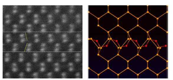
Seen directly in STEM
The MST layer perturbs the silicon lattice locally
Left: scanning transmission electron microscope image; between the dashed lines the atomic columns shift (yellow) where the partial oxygen monolayer sits. Right: the matching atomic model, oxygen in red. Above and below, the lattice is ordinary silicon.
The local perturbation is validation of the atomistic modelSTEM courtesy of Prof. G. Balakrishnan and M. Frost, University of New Mexico.
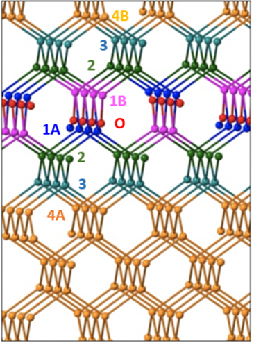
| Atom | Layer / site | Site charge |
|---|---|---|
| Oxygen | O | −1.01 |
| Silicon | 1A | +0.67 |
| Silicon | 1B | +0.51 |
| Silicon | 2 | −0.07 |
| Silicon | 3 | −0.01 |
| Silicon | 4A | 0.00 |
| Silicon | 4B | 0.00 |
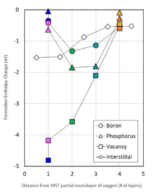 Defects and dopants all sit lower in energy near the MST layer, so they are held there rather than diffusing through.
H. Takeuchi et al., IEEE IMFEDK 2022.
Manufacturing
Each MST film is custom-engineered for its application
Tool-independent
MST deposition is independent of tool supplier and chamber type.
Proven know-how
Perfected over hundreds of Silicon and Device wafer runs
Straightforward install
Existing reactors run MST with a simple upgrade.
Thermally stable
MST films have proven thermal stability.
Manufacturing Tools
Proven MST growth on EPI tool of all three vendors
MST has been grown in-situ in production proven epitaxial reactors from the major tool suppliers. The upgrade requires feeding MST precursor that is readily available from chemical suppliers.
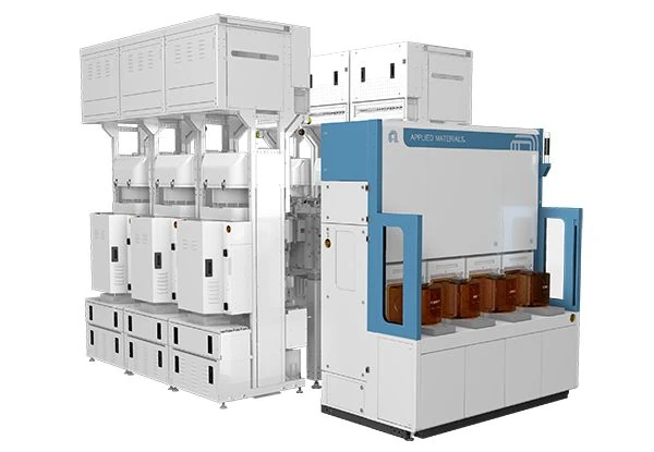
Applied Materials
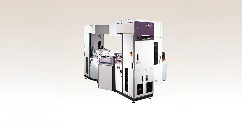
ASM
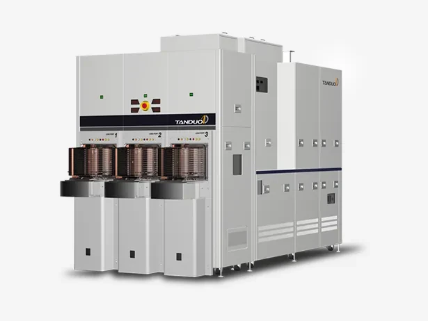
Kokusai Electric

Work with us
Partner with Atomera
Evaluate MST in your own process and devices with Atomera's engineering team.
Contact us