

Applications
Application
Wafer Thinning Etch Stop
A thick P⁻ epi layer on a P⁺ substrate with a sharp interface, so wafer thinning and wet etch stop cleanly.
How MST helps
MST blocks boron diffusing up from the P⁺ substrate during thick, high-temperature epi growth. The P⁻/P⁺ interface stays sharp, giving a clean stop for wafer thinning and etch-back.
Learn more: whitepapers & publications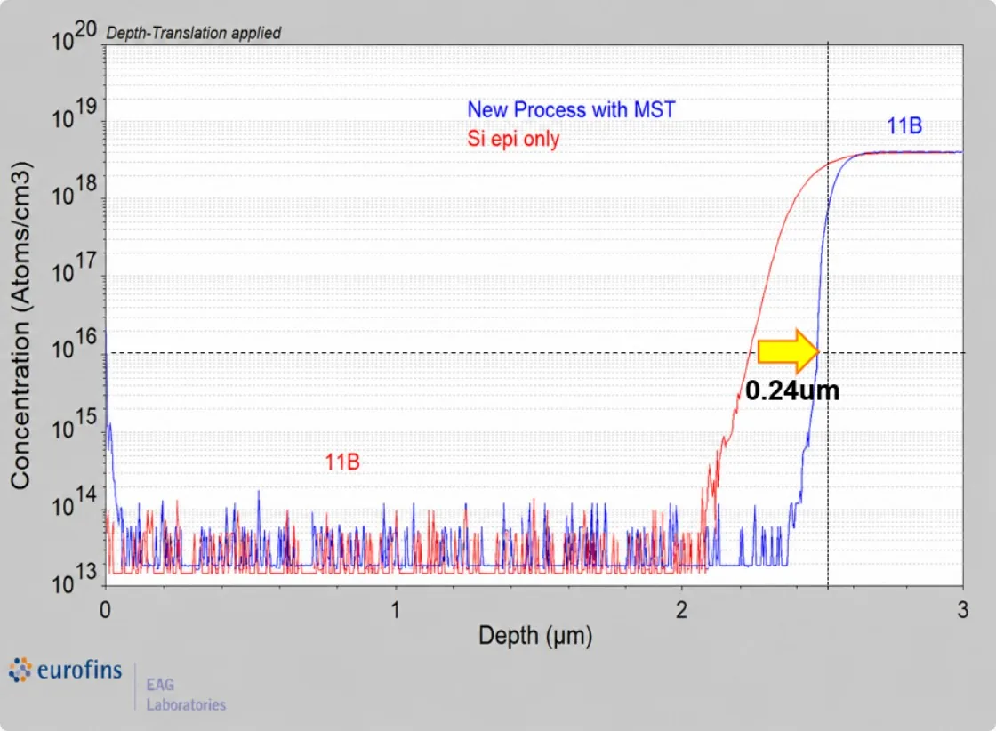
Silicon data
A 9× sharper P⁻/P⁺ transition
2.5 µm P⁻ epi grown at 1050 °C on a P⁺ substrate, with and without MST first. Initial demonstration on 200 mm wafers.
0.27 → 0.03 µm
transition-layer thickness between the P⁻ epi and the P⁺ substrate
0.24 µm
closer to the design depth at 10¹⁶ cm⁻³ boron

Work with us
Partner with Atomera
Evaluate MST in your own process and devices with Atomera's engineering team.
Contact us